| Go To: A B C D E F G H I J K L M N O P Q R S T U V W X Y Z |
| Active Components: |
Semiconductor devices, such as transistors and diodes, that can change its basic characteristics in an powered electrical circuit, such as amplifiers and rectifiers. |
| Advanced Substrates: |
Printed circuit board materials with superior thermal properties for products requiring high-frequency transmission. |
| Analog Circuit: |
An electrical circuit that provides a continuous quantitative output as a response from its input. |
| Annular Rings: |
The conductive copper rings around the holes in a printed circuit board. |
| AOI: |
Automatic Optical Inspection uses technology to inspect an object. |
| Artwork: |
The design of a circuit board. |
| Assembly File: |
A drawing indicating where components are placed on a PCB. |
| Backplanes or Backpanels: |
Multi-layer printed circuit boards typically used to connect other boards. |
| Ball Grid Array (BGA): |
When solder ball interconnects cover the bottom surface of a package. |
| Bare Board: |
An unpopulated PCB. |
| Bill of materials (BOM): |
A detailed list of all the necessary subassemblies, components, and raw materials for an assembly. |
| Blind or Buried Vias: |
Holes within complex pcbs which connect inner layers. |
| Board Cleaner: |
A production line machine used to remove solder residue and other foreign material acquired during assembly from the PCB. |
| Built-In Self Test: |
An electrical testing method that enables devices to test themselves. |
| Burn-In Testing: |
A product functionality test that powers products for an extended period of time. |
| BUS: |
Electrical connections between integrated circuits and peripheral semiconductors. |
| CAD: |
Computer Aided Design. |
| CAM Files: |
Files provided for manufacturing PCB. |
| CAM: |
Computer Aided Manufacturing. |
| Capacitors: |
Simple, non-semiconductor electrical components. |
| Ceramic Ball Grid Array (CBGA): |
A ball grid array package with a ceramic substrate. |
| Chip Scale Packaging: |
A way of packaging integrated circuits without using epoxy that takes up less board space. |
| Chip: |
An individual circuit or component. |
| Chip-On-Board (COB): |
The process of using a wire bond, solder or other conductive adhesives to attach chips onto printed circuit boards. |
| Coating: |
A thin layer deposit on a substance surface. |
| Coefficient of Thermal Expansion (CTE): |
The ratio of dimensional change of an object from the original dimension when temperature changes. |
| Component Side: |
The side of a printed circuit board which has the most mounted components. |
| Contact Angle (Wetting Angle): |
The angle created on the contact surfaces when two objects are bonded together. |
| Copper Foil (Base Copper Weight): |
Coated copper layer on the board measured by weight or thickness. |
| Curing Time: |
The time needed for an epoxy to fully cure at a given temperature. |
| Curing: |
The process of polymerizing a thermosetting epoxy. |
| Design For Manufacturability (DFM): |
An initial process to determine the feasibility of creating electronic products. |
| DFSM: |
Dry Film Solder Mask |
| Die Bonder: |
The machine placement of IC chips onto a chip-on-board substrate. |
| Die: |
An integrated circuit chip cut from a finished wafer. |
| Dielectric: |
The insulating medium between conductors. |
| Double-Sided Assembly: |
PCB assembly with components on both sides of the board. |
| Edge Clearance: |
The smallest distance from any conductors or components to the edge of the PCB. |
| Edge Connector: |
A connector on the circuit-board edge used to connect to other circuit board or electronic device. |
| Environmental Stress Screening: |
A way for detecting defects using extreme high and low temperatures and/or voltages. |
| ESR: |
Electro-statically applied solder resist. |
| Fine Pitch: |
Used when referring to surface-mount components with a lead pitch of 25 mils or less. |
| Finger: |
A card-edge connector. |
| Flex Circuit Assembly: |
A way of attaching electrical components to a flexible circuit. |
| Flip Chips: |
Structures that use solder bumpers without leads to hold interconnected circuits face down on a pcb with solder bumpers without leads. |
| Flux: |
The material used to remove oxides from metal surfaces. |
| Functional Test: |
Testing an assembled device by simulating actual use. |
| Gerber File: |
Data file used to control a photoplotter. |
| GI: |
Woven glass fiber laminate with polyimide resin. |
| Ground Plane: |
The common ground reference in a multilayer PCB for current returns and shielding. |
| HDI: |
High Density Interconnect. |
| Hermetic: |
Airtight sealing of an object. |
| Hole Density: |
The number of holes per unit area on a PCB. |
| In-Circuit Test: |
The testing of specific components or parts of a circuit rather than testing the whole circuit. Used for early-stage defect detection. |
| Interstitial Via Hole: |
An embedded through-hole that connects two or more conductor layers in a PCB. |
| Laminate: |
A composite material created by bonding several layers of same or different materials together. |
| Lamination: |
The process creating laminate using pressure and heat. |
| Laser Direct Imaging: |
A method that increases board density with laser technology. |
| Leakage Current: |
A small amount of current that flows across a dielectric area between two adjacent conductors. |
| Legend: |
Printed letters or symbols on the PCB indicating important information like part numbers or company identification. |
| LPI: |
Liquid Photo-Imageable solder mask. |
| Magazine: |
A portable enclosure used to hold PCBs or product. |
| Micro Ball Grid Array: |
The process for placing an integrated circuit or other component on a multi-layer pcb using an array of extremely small solder balls (or columns) at each contact. |
| Microprocessors: |
Integrated circuits that contain the CPU for a computing device. |
| Microvias: |
Laser-created small holes, or vias. |
| Minimum Conductor Width: |
The smallest distance between any two adjacent conductors, such as traces, in a PCB. |
| Multi-Chip Module Laminates: |
A pcb design for placing multiple integrated circuits or other components on a limited surface area. |
| Multilayer PCB: |
Circuit boards with three or more layers of printed circuits separated by laminate layers and bonded together with internal and external interconnections. |
| NC Drill: |
A numeric control drill used to drill holes at exact locations. |
| Netlist: |
List of parts and their connection points. |
| Node: |
A pin or lead to which at least two components are connected through conductors. |
| NPTH: |
Non-plated trough-hole. |
| Pad: |
The pattern indicating the appropriate connection and attachment of electronic components on the PCB. |
| Pallet / Carrier: |
A frame used to hold a PCB during assembly. |
| PCB: |
Printed Circuit Board. |
| PEC: |
Printed Electronic Component. |
| Pick
& Place Machine: |
Automatically "picks"
components from a supply and "places" them on the PCB in the correct location. |
| Pick-and-Place |
An assembly process in which components are selected and placed onto specific locations according to the assembly file. |
| Pin-Through-Hole (PTH) |
A method of fusing low-density components to a printed circuit board using pin-through-hole connections. |
| Pitch |
The center-to-center spacing between conductors on a PCB. |
| Plating Resist |
Material used on an area to prevent plating. |
| PLC |
Programmable Logic Controller (Simple Computer) |
| Printed Circuit Board (PCB): |
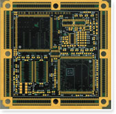
Made from insulating, non-conductive material, this board has metal tracks which connect soldered on devices and components. |
| Product Assembly And Test: |
The process of placing components on printed circuit boards using surface mount and through-hole technologies. |
| Prototyping: |
The processes of building a small quantity to test and verify design before production. |
| PTH (plated-throughhole): |
A plated hole providing connectivity between different layers or sides of a PCB. |
| Reflow Soldering: |
Applying heat to a pcb with the purpose of melting existing solder past and rejoining metal layers. |
| Resist: |
Material used to mask or to protect certain areas of a pattern from etching, solder, or plating. |
| Route (or Track): |
The layout or wiring of an electrical connection. |
| Scanning Electron Microscopy: |
A method of scanning that uses a microscope with 200 times magnification or greater. |
| Screen Printing: |
The method of transferring an image from a patterned to a board by forcing paste through a screen printer. |
| Semiconductors: |
Materials whose properties fall between those of insulators and conductors, and is also the term used for all electronic components made from semiconductor material. |
| Silk Screen(Silk Legend): |
The epoxy-ink legend printed on PCB. |
| Small Outline Integrated Circuit (SOIC): |
An integrated circuit with two parallel rows of pins in surface mount package. |
| SMD: |
Surface Mount Device. |
| SMOBC: |
Solder mask over bare copper. |
| SMT: |
Surface Mount Technology. |
| Solder Bridging: |
Using solder to connect two or more adjacent pads to form a conductive path. |
| Solder Bumps: |
Round solder balls used in face-down bonding. |
| Solder Mask: |
Coating to prevent solder to deposit on. |
| Solder Wick: |
A band of wire is used to remove solder. |
| Surface Mount Technology (SMT): |
A flexible technology used to solder electrical components directly to a board. |
| Tape AutomatedBonding: |
An assembly process involving the application of components onto a circuit board using temperature and pressure. |
| Temperature Coefficient (TC): |
The ratio of a quantity change of an electrical parameter of an electronic component from its original value when temperature changes. |
| Test Point: |
A specific point on a circuit board used for functionality or quality testing. |
| Three-Dimensional Laser Paste: |
An inspection method using microscopes with lasers. |
| Through Hole Process |
A method of soldering where components are first placed in holes in the PCBs at points where they are to be soldered. The hole is then filled with solder to complete the process. |
| Transfer |
Movement of product into, across, and then out from the machine conveyor. |
| Transfer Conveyor |
Incorporates intelligent control like a PLC (Programmable Logic Controller) or computer to control the movement of boards or product. |
| Transfer Workstation |
An Edge Carry or Flat Belt conveyor that incorporates a work surface, light and shelf for easy human interface with product as it passes on the line. |
| Turn-key |
An outsourcing model which turns all aspects of electronics manufacturing over to an EMS provider, who buys the raw materials and components and bills the OEM for a complete assembly. |
| UL: Underwriters Laboratories |
A popular safety standard for electrical devices supported by many underwriters. |
| Via |
A plated-through hole used for interconnection of conductors on different sides or layers of a PCB. |
| Wave Soldering |
A manufacturing operation in which solder joints are soldered simultaneously using a wave of molten solder. |
| X-Ray Laminography |
An inspection method that uses x-rays to view thin layers of a circuit board. |
